Through Glass Via: Next Gen Advanced Electronics Packaging

As the demand for AI, high-speed computation and powerful computing continues to grow, there is an increasing need to enhance the number of transistors in a single package. However, traditional organic materials like silicon, commonly used for interposers, are encountering limitations. Glass substrates offer numerous advantages, including exceptional flatness, high thermal stability and rigidity. These attributes enable the miniaturisation and integration of transistors on a glass substrate.
E&R Engineering has dedicated a self-developed accelerated optics solution (ACES) combined with advanced laser technology to delivering total solutions for glass substrates for several years, including through glass via (TGV), laser glass polishing and multi-beam path laser cutting solutions for glass.
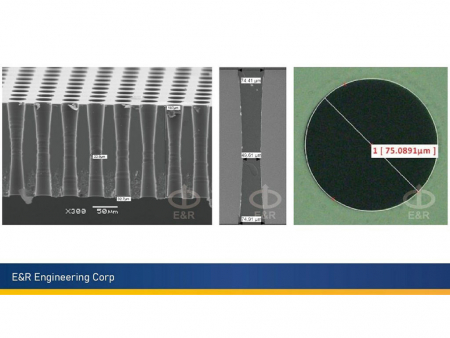
TGV, an essential method for glass substrates to achieve 2.5D/3D packaging, involves internal modification for subsequent wet etching processes. Currently, the most common TGV method uses a filamentation beam to generate multiple shots for internal modification, with a VPS of approximately 50 vias per second only. However, E&R has opted for a Bessel beam system as ACES and laser total solution, which significantly increases the accuracy.
E&R's full automation TGV tool can handle glass panels up to 600mm by 600mm, with a thickness of up to 1,100µm, while achieving a good aspect ratio of 1:10. The via diameter can be controlled from 50 to 200µm with a defect-free sidewall, of which the roughness can achieve ≤1µm after etching.


